Fig. 22.1
Three-dimensional cutaway view of our 1,310 nm MEMS-VCSEL. InP gain region and GaAs mirror are integrated by wafer bonding. VCSEL is optically pumped at 980 nm (From Ref. [19])
Figure 22.2 illustrates a similar view of a 1,050 nm device. Here, the gain region employs compressively strained indium gallium arsenide (InGaAs) quantum wells integrated with a GaAs/AlxOy fully oxidized mirror. The structure requires no wafer bonding, since the InGaAs quantum wells are nearly lattice matched to the underlying GaAs and can be integrated by epitaxial growth with the GaAs-based mirror. In this case, the optical pump is at 850 nm, generating tunable 1,050 nm emission.
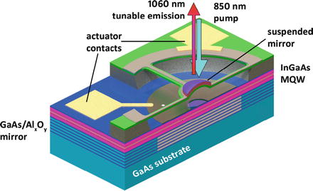

Fig. 22.2
Three-dimensional cutaway view of 1,050 nm MEMS-VCSEL. The structure is grown in one epitaxial step with no wafer bonding. VCSEL is optically pumped at 850 nm (From Ref. [18])
Implicit in the device structures of Figs. 22.1 and 22.2 are a number of design choices that are critical to obtaining wide tuning range. Below, we briefly describe those choices and the justification for each.
22.2.2 Optical Versus Electrical Pumping
This effort to date has focused on optically rather than electrically pumped devices. Though the ultimate low-cost device will be electrically pumped, optical pumping provides a number of performance advantages over electrical pumping, including enhanced tuning range and spectral purity, for a variety of reasons. First, the absence of electrically active dopants reduces absorption losses and thus reduces threshold gain, enabling lasing over a wider portion of the available gain spectrum. Second, the absence of resistive heating associated with electrically pumped devices also increases available gain and again promotes wide tuning range. Third, optical pumping eliminates the need for thick intracavity current-spreading layers, which extends the overall cavity length, reducing the cavity free spectral range (FSR) and ultimately limiting the laser tuning range. The widest previously reported MEMS-VCSELs have had tuning range limited by (FSR) [15, 24]. Fourthly, optical pumping simplifies the use of resonant periodic gain structures, which are known to provide a maximal gain enhancement in a VCSEL cavity [25]. Lastly, a single-spatial-mode pump laser provides an optimal overlap between the pump area and the lowest order spatial mode of the VCSEL, which suppresses lasing of unwanted transverse modes. This enables very high side mode suppression ratio (SMSR) of >45 dB to be routinely achieved in properly designed optically pumped devices. This high SMSR has a favorable impact on SS-OCT imaging quality.
We also note that the highest power tunable VCSELs have been demonstrated by optical pumping, achieving an impressive peak power of 14 mW near 1,550 nm [15]. This falls short by a factor of 2–3 from that required for SS-OCT near 1,310 nm but is somewhat close to power levels required for ophthalmic imaging at 1,050 nm. Our design philosophy in this effort is to design the MEMS-VCSEL itself for wide tuning range, enabling improved axial resolution, rather than high output power. We then amplify the VCSEL emission with a semiconductor optical amplifier. The resulting widely tunable, high power emission is used as the source for OCT imaging and has resulted in excellent images, as discussed in Sect. 22.6 below and in additional publications. The previous high power result at 1,550 nm [15], however, suggests that further engineering of 1,050 nm MEMS-VCSELs may remove the need for amplification at this wavelength.
22.2.3 Mirror Design
Wide mirror reflectivity bandwidth is critically important for wide tuning range. A high refractive index contrast mirror with a short optical field penetration depth is also critical to reduce the overall effective cavity thickness and increase the FSR, which further increases tuning range. The fully oxidized mirror shown in Figs. 22.1 and 22.2 satisfies these requirements better than virtually any other mirror, with the possible exception of a hybrid metal/deposited dielectric mirror [24], which we discuss briefly below. Wide bandwidth is also provided by the recently proposed and demonstrated high contrast grating (HCG) [11]. The HCG provides a high reflectivity in a thin single layer structure that has a strong lateral refractive index perturbation. This provides very low mass and high mechanical resonance, but the calculated HCG bandwidth [26] falls short of the fully oxidized mirror, and the ability of the HCG to provide >30 nm tuning in a VCSEL structure remains unproven.
The fully oxidized mirror is realized by starting with an epitaxially grown stack of GaAs/AlAs, etching holes or mesas into the epilayer structure to access the underlying AlAs layers, and exposing the material to a steam atmosphere at elevated temperature [23]. This converts the AlAs layers to AlxOy layers with a refractive index around 1.55, providing a large index contrast relative to the surrounding GaAs layers (index around 3.4). This enables the incorporation of a high reflectivity, wide bandwidth, and short penetration depth end mirror.
The use of the fully oxidized mirror at 1,050 nm is a natural choice, since it can be epitaxially grown with the GaAs gain region. Its use at 1,310 nm is less obvious, since this necessitates wafer bonding an InP-based gain region to a GaAs-based mirror region, as shown in Fig. 22.1. The choice of a heterogeneously integrated material structure stems from the fact that the InP material system provides no easily oxidized material-like AlAs or any other epitaxially grown high-index contrast mirror option [27]. In response to this challenge, previous MEMS-tunable work at 1,550 nm has employed deposited dielectric and/or metal/dielectric mirrors on both sides of the cavity [15, 24]. Similar approaches could be employed at 1,310 nm. Our choice of the wafer-bonded semiconductor mirror is related to mechanical robustness, manufacturability, and ease of handling, relative to a process that requires either backside vias [15] or gold bonding to a transfer substrate [24]. In addition, the transparency of the fully oxidized mirror enables coupling light out at either side of the cavity, to satisfy the needs of a variety of applications, while the metal/dielectric mirror can only function as a back mirror.
Figures 22.3 and 22.4 illustrate the reflectivity of three candidate mirrors for widely tunable MEMS-VCSELs centered at 1,300 nm, neglecting absorption and scattering losses. Reflectivity is calculated with respect to the antireflection (AR)-coated gain medium (i.e., looking from the gain medium outward to the respective mirrors), assuming that the pure dielectric mirror is suspended, and the fully oxidized or hybrid mirror is the fixed back mirror. Both the fully oxidized mirror (GaAs/AlxOy) and hybrid dielectric/gold mirror (AlF3/ZnSe/Au) show a reflectivity bandwidth between first nulls of about 800 nm. The suspended dielectric mirror bandwidth between nulls is about half this value. The reflectivity plot of Fig. 22.4 shows the reflectivity spectrum of the same three mirrors over the same wavelength range but only for reflectivity above 99 %. Efficient top-emitting VCSELs require >99.9 % reflectivity on the back mirror. The fully oxidized and the hybrid dielectric/metal mirror both satisfy this requirement over >400 nm, with again the hybrid mirror exhibiting a slightly wider bandwidth. A lower reflectivity pure dielectric mirror, such as the SiO2/TiO2 combination calculated in Figs. 22.3 and 22.4, functions as the output coupler. Requirements on this output coupler are somewhat relaxed relative to the back mirror, with a required reflectivity in the range of about 99.5 % < R < 99.9 %. Reflectivity lower than 99.5 % increases the required threshold gain or inhibits wideband lasing, and reflectivity > 99.9 % can compromise output power as very little light is coupled out of the optical cavity. The SiO2/TiO2 combination shown in the figure satisfies this requirement over about 200 nm bandwidth, as do other commercially available and robust dielectric coatings such as SiO2/Ta2O5 or SiO2/Nb2O5.
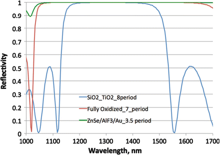
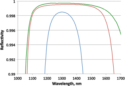

Fig. 22.3
Reflectivity of two candidate back mirrors (red and green) and one suspended mirror (blue)

Fig. 22.4
Reflectivity in range > 99 %. Back mirrors (red and green) provide > 99.9 % over 400 nm. Suspended (blue) shows 99.5 % < R < 99.9 % over ∼200 nm
A MEMS-VCSEL employing the dielectric mirror shown in Figs. 22.3 and 22.4 as an output coupler, and either of the back mirrors shown, can be expected to support lasing over 100–200 nm tuning range near 1,310 nm. Similar reflectivity plots can be generated near 1,050 nm and similar conclusions formed. The ultimate limit on tuning then becomes the cavity free spectral range (FSR) or the available gain bandwidth. In previous electrically pumped MEMS-VCSELs, FSR has often limited tuning range. In our optically pumped devices, we have pushed the FSR to 161 nm at 1,310 nm, achieving 150 nm tuning range as discussed below [19]. Achievement of this tuning range requires not only wide mirror bandwidth and large FSR but also proper engineering of the active region. We briefly discuss the active region material design in the next section.
22.2.4 Active Region Material Design
As discussed earlier, MEMS-VCSELs at both 1,050 and 1,310 nm employ compressively strained multi-quantum well (MQW) active regions, since compressive strain provides gain enhancements in quantum well gain for both GaAs-based (1,050 nm) and InP-based (1,310 nm) multi-quantum well active regions [28, 29]. Tensile strain has also been shown to provide superior edge-emitting laser performance for InGaAsP/InP MQW devices [30], but tensile strain enhances transverse magnetic (TM) gain (electric field perpendicular to quantum well plane) rather than transverse electric (TE) gain [29]. Since light propagation is perpendicular to the plane of the quantum well in VCSELs, the electric field will be in the plane of the quantum well and thus compressively strained wells can be employed.
MEMS-VCSELs at 1,050 nm employ InGaAs quantum wells with GaAs barriers as the gain region. This material is known to provide higher gain relative to lattice-matched quantum wells on GaAs [29], and incorporation of indium is necessary to increase the wavelength on GaAs beyond the ∼870 nm achievable with lattice-matched materials. Compressively strained InGaAs quantum wells have been used for 980 nm fixed wavelength VCSELs since early in the history of VCSELs [31], and more recently, fixed wavelength devices at 1,100 nm using strained InGaAs quantum wells have also been demonstrated [32]. MEMS-VCSELs at 1,310 nm employ compressively strained AlInGaAs/InP quantum wells. Although the compressively strained InGaAsP/InP quantum wells have a longer history in edge-emitting lasers [30], the AlInGaAs/InP material system has provided superior temperature performance in edge-emitting lasers at 1,310 nm [33]. Other demonstrations in both 1,550 nm fixed wavelength [34] and 1,550 nm MEMS-VCSELs [35] have employed compressively strained AlInGaAs/InP multi-quantum well active regions. For tunable VCSELs, a lesser-known advantage of the AlInGaAs/InP material system is the wider gain spectrum relative to InGaAsP/InP. This width can be obtained by designing quantum wells to have two confined quantum states. State separation is wider in the AlInGaAs/InP material system relative to the InGaAsP/InP system, because of the larger conduction band offset [33], leading to wider gain spectra and higher output powers. This has been demonstrated in superluminescent diodes (SLED) developed by Praevium Research, an example spectrum of which is shown in Fig. 22.5. The InGaAs/GaAs system is also capable of wide dual-quantum state gain spectra, as shown in the SLED spectrum of Fig. 22.6.
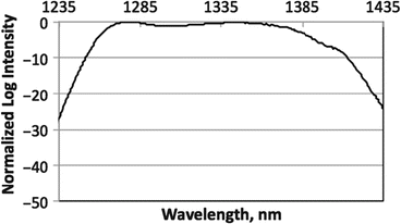
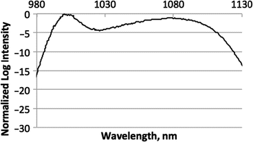

Fig. 22.5
Emission spectrum from a 1,310 nm superluminescent diode (SLED) using an AlInGaAs/InP MQW design with two quantum states. Width of SLED spectrum is indicative of width of the gain spectrum

Fig. 22.6
Emission spectrum from 1,050 nm superluminescent diode (SLED) using an InGaAs/GaAs QW structure with two quantum states. Width of SLED spectrum is indicative of width of the gain spectrum
22.2.5 MEMS Actuator Design
For SS-OCT operation, the ideal MEMS actuator should have a flat and wide bandwidth frequency response, enabling operation at arbitrary scan rates and linearization of drive waveforms through control of higher frequency dynamics. Note that here we focus exclusively on electrostatic rather than electrothermal [24] actuation, since the latter does not provide speeds appropriate for SS-OCT. Numerous parameters associated with the actuator geometry affect the MEMS-VCSEL tuning frequency response. For the specific geometry of Figs. 22.1 and 22.2, using a central plate with a number of supporting arms, important parameters include the thickness and stress level of the membrane layer, the overall actuator area, the length and width of the supporting arms, the number of arms, the diameter of the central distributed Bragg reflector (DBR) mirror, and the initial air gap. These parameters affect resonant frequency, damping, resulting bandwidth, voltage required for a given wavelength shift, and maximum achievable wavelength span. Many of these factors must be traded off to achieve a commercially viable design. For example, increasing the thickness and stress of the membrane layer increases the resonant frequency but may require impractical voltages to achieve the full tuning range. Increasing the initial air gap thickness increases maximum achievable static deflection, because tuning beyond about one-third of the initial air gap causes electrostatic forces to overwhelm restoring forces, leading to “snapdown” of the actuator [36]. In dynamic operation, the peak voltage can exceed the snapdown voltage as long as the actuation frequency is sufficiently high. Nevertheless, a certain amount of static bias is required on all devices, and avoiding snapdown in electrostatic actuators therefore remains an important design consideration. However, increasing the initial air gap thickness also reduces the free spectral range, which reduces maximum achievable tuning range. Thus, an optimum initial air gap thickness must be chosen.
Diameters of the central DBR mirror and overall actuator area impact performance in a variety of ways. Minimizing DBR diameter increases resonant frequency through reduced mass, but diameter must be larger than the mode size to minimize sidewall scattering losses, accounting for lithographic fabrication tolerances on the alignment between the DBR and the central axis of the cavity. Increasing the overall area of the actuator can either increase or decrease resonant frequency, since increased mass is competing with increased spring stiffness. Lastly, increasing area increases squeeze-film damping through interaction with viscous air [37], which can reduce resonator Q and flatten frequency response, as long as the device is not overdamped.
Figure 22.7 illustrates the range of frequency responses experimentally measured, through variation of the parameters discussed above. As shown, resonant frequencies vary from about ∼300 to ∼500 kHz, and damping varies from highly under-damped to near critically damped. Peak voltages for full tuning over one FSR (see results in Sect. 22.4 below), for all designs shown, are under 85 V. The flatter responses with 300–500 kHz resonance are preferable for linearizing the wavelength tuning response, as discussed in Sect. 22.5 below. The highest resonance devices have led to record axial line rates of 1.2 MHz [20], when both forward and backward wavelength scans are employed.
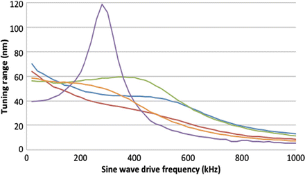

Fig. 22.7
Various frequency responses achieved through modification of the actuator geometry and membrane stress
The geometry of the MEMS actuator is sufficiently complex that the qualitative tradeoffs discussed above must be accurately modeled using a 3-D finite-element tool such as COMSOLTM to accurately predict frequency response and modal behavior. Finite-element modeling also identifies some subtle features such as the impact of higher order modes on the dynamic response of the actuator. Figure 22.8 illustrates example COMSOLTM modeling of a typical suspended mirror. The model reveals a lowest order “piston” mode, which is the primary peak seen in the responses of Fig. 22.7, and the motion desired for VCSEL tuning. Additionally shown is an undesirable tilting mode and another undesirable mode corresponding to movement of the actuator arms with minimal movement of the central plate. These higher order modes can be excited by fabrication imperfections or higher drive harmonics used for linearization, but their impact can be minimized by increasing the damping in the structure. Advanced MEMS characterization tools such as laser Doppler vibrometry (LDV) [38, 39] can help visualize actuator movement in real time, correlate with theoretical models, and adjust fabrication methods as necessary to achieve the desired movement. Figure 22.9 illustrates one frame of an LDV movie of actuator motion for a 4-arm device. Depressions in the central plate are measurement artifacts arising from transparent portions of the oscillating membrane. The primary value of the movie from which this frame is constructed is a demonstration that the actuator is moving primarily in the desired “piston mode,” rather than in undesirable higher order modes.

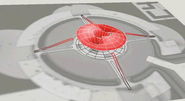

Fig. 22.8
COMSOLTM modeling of the three lowest order modes of a 4-arm actuator, illustrating piston mode (a), tilt mode (b), and higher order mode with minimal plate motion (c)

Fig. 22.9
Single frame of laser Doppler vibrometer (LDV) animation of actuator motion. Depressions in central plate are artifacts resulting from transparent portions of the membrane. The overall actuator motion is in the primary desired piston mode
22.3 Widely Tunable VCSEL Fabrication
Figures 22.10a–l illustrate key elements of the process flow used to fabricate the device structures illustrated in Figs. 22.1 and 22.2. Many elements of the process flow are derived from previous work [40]. The general process flow is essentially identical for 1,050 and 1,310 nm devices, with the exception that 1,310 nm devices additionally require wafer bonding to combine the InP-based epitaxial structure with the GaAs/AlxOy bottom mirror prior to beginning MEMS-VCSEL fabrication. In addition, thicknesses and composition of epitaxial layers and dielectric films are different for the two wavelengths.
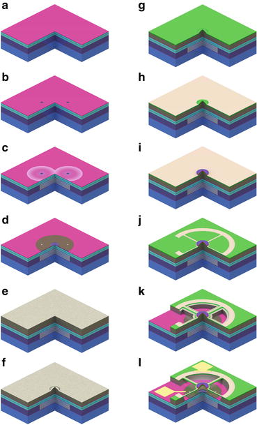

Fig. 22.10
MEMS-VCSEL fabrication. (a) Initial structure with gain region (pink) on top of the fixed bottom mirror. (b) Two etched oxidation vias. (c) The oxidized mirror layer region forms a figure 8 around the oxidation vias. (d) Deposited bottom contact (brown disk) and AR coating (purple central film). (e) Sacrificial layer (gray top) deposited over entire structure. (f) Curved surface etched in center of laser aperture. (g) Dielectric membrane (green) deposited over the entire sample. (h) Tan top metal deposited over membrane with central opening for light passage. (i) Dielectric top mirror (purple) deposited and patterned over central device area. (j) Actuator pattern wet-etched into tan top metal. (k) Actuator pattern is transferred to underlying layers. (l) Final structure including deposited contact pads (yellow) and undercut sacrificial layer creating a suspended membrane
For 1,310 nm devices, the process begins with wafer bonding of an epitaxially grown multi-quantum-well gain region on an InP wafer to an epitaxially grown stack of GaAs/AlAs layers on a GaAs wafer. After bonding, the InP substrate is chemically etched away, leaving an InP gain region integrated on a GaAs substrate. Wafer bonding is a well-known process in which lattice-mismatched semiconductors, such as GaAs and InP, can be joined through application of pressure and heat [41]. Wafer bonding for VCSELs was first demonstrated in the mid-1990s and led to some of the first demonstrations of 1,310 nm fixed wavelength VCSELs [42].
After bonding, 1,310 and 1,050 nm device processing proceeds identically as shown in Fig. 22.10a–l. Figure 22.10a shows the initial epitaxial structure, with gain region integrated on the GaAs/AlAs mirror layers. Figure 22.10b illustrates the formation of two oxidation via holes, which provide access to the underlying mirror layers for a subsequent oxidation step. The etched structure is then exposed to a steam atmosphere at elevated temperature, converting AlAs to AlxOy, creating a high contrast mirror in combination with the high-index GaAs layers. Figure 22.10c illustrates this mirror oxidation step, where the oxidized region expands radially around the etched holes, forming a figure 8 pattern. Deposition of the bottom contact layer proceeds after oxidation, containing an apertured central region with a broadband antireflection (AR) coating (Fig. 22.10d), through which intracavity light will pass into an air gap. Next, a sacrificial layer is deposited (Fig. 22.10e), the thickness of which determines the initial air gap and zero-bias device wavelength. In step (Fig. 22.10f), a curved surface is formed on the sacrificial layer through pattern transfer of a reflowed resist mesa. This curved surface contributes to the formation of a half-symmetric cavity in the final device. Figure 22.10g illustrates deposition of a dielectric membrane layer (green) on the sacrificial layer, followed by deposition of an apertured top actuator contact metal in Fig. 22.10h. The aperture serves to allow passage of light through the structure.
Deposition of the top dielectric DBR proceeds next, followed by etching of a post in the DBR (purple central region) to expose the top contact metal in the field (Fig. 22.10i). Wet chemical etching of the top contact metal creates the desired actuator shape, as shown in Fig. 22.10j. Further dry etching transfers this geometry downward through dielectric and sacrificial layers (Fig. 22.10k). After deposition of top and bottom wire bond pads, chemical undercutting of the sacrificial layer creates the final suspended structure shown in Fig. 22.10l.
22.4 1,310 nm and 1,050 nm VCSEL Static and Dynamic Tuning Results
22.4.1 Section Overview
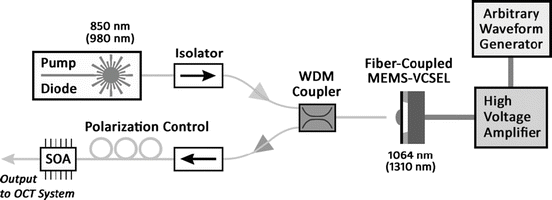
This section describes the static and dynamic tuning range obtained with various generations of both 1,310 and 1,050 nm MEMS-VCSELs. Section 22.5 discusses additional laser properties relevant to OCT imaging, and Sect. 22.6 shows representative images obtained with these devices. Figure 22.11 illustrates a schematic of the optically pumped MEMS-VCSEL source used for OCT imaging, along with the supporting elements around the VCSEL source. An incoming optical fiber is coupled to the MEMS-VCSEL cavity, delivering incoming pump light at 980 nm for 1,310 nm MEMS-VCSEL operation and at 850 nm for 1050 nm MEMS-VCSEL operation. Isolators protect both the pump lasers and the MEMS-VCSELs from back reflections, ensuring low noise operating and enhancing laser lifetime. The pump fiber also collects the emitted tunable VCSEL radiation, and a subsequent WDM coupler separates the incoming pump light from the outgoing MEMS-VCSEL emission, with the latter sent to a semiconductor optical amplifier (SOA). The amplified VCSEL emission (output of the SOA) is sent to the OCT imaging system. As shown, the VCSEL output passes through a fiber polarization controller in order to align the polarization to the preferred orientation for maximum gain through the polarization-dependent SOA. Both pre-amplified and post-amplified VCSEL emissions are sent to an optical spectrum analyzer (not shown) to generate the tuning results below. Both static and high-speed time-dependent tuning voltages are applied via a high-voltage (HV) amplifier, which is driven by an arbitrary waveform generator.

