Fig. 14.1
Block diagram of an individual C66x DSP core
The instruction set also includes single instruction, multiple data (SIMD) format. SIMD is often used for vector data processing where the same processing (multiplication, addition, etc.) can be done in parallel on multiple input datasets producing multiple output datasets. This architecture allows up to 128-bit vector processing. The 128-bit vector can hold up to four single precision numbers in IEEE754 format. The M unit can do four single precision multiply operations per cycle. Each of L and S can do two single precision additions per cycles. The two sets of L, S, and M can then do eight single precision multiply-add operations per cycle (i.e., 16 floating-point operations or FLOP per cycle). There is also the ability to do double precision operations as well as integer operations of various widths (8 bit or byte, 16 bit or half word, and 32 bit or full word). Various mixed mode operations are also allowed.
There are two general purpose register files, one on each side, which feeds data to the units of that side. There is also a cross connect so that units on one side can use the data from the units on the other side. The art of efficient programming a VLIW engine like the C66x DSP core lies in the ability to feed as many instructions as possible to the parallel units without overwhelming the registers. Fortunately, a large amount of the standard signal and image processing functions is available as standard libraries, and the user would not need to write optimized functions for these.
The overall block diagram of the TMS320C6678 DSP with eight cores is shown in Fig. 14.2. In addition to the eight cores, the device comes with a rich set of standard interfaces like PCI express, Serial Rapid I/O (SRIO), and gigabit Ethernet.
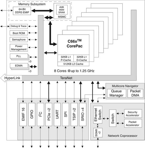

Fig. 14.2
Block diagram of the eight-core TMS320C6678 DSP
14.3.1 Memory Hierarchy
The memory hierarchy available in a particular processor is an important design consideration for embedded processors. The TMS320C6678 DSP has 32 KB of L1 program (L1P) and 32 KB of L1 data (L1D) cache memory, as well as 512 KB of L2 cache memory per core, integrated in the chip. Unlike a conventional CPU, both L1 and L2 memory in the TMS320C6678 can be configured as RAM or cache or part cache/part RAM. This flexibility is exploited in this implementation of the OCT signal chain. In addition to this per-core memory, the device also integrates 4,096 KB of multi-core shared memory (referred to as MSMC). This part of the memory is accessible by all the cores.
All L2 memory incorporates error detection and error correction which acts as auto fault detection and correction for device and memory errors. This may be an important aspect in safety critical applications like medical imaging devices. The device includes 64-bit DDR3 external memory which runs at 1,333 MHz, giving a maximum DDR3 (with error correction DRAM support) bandwidth of about 10.6 GB/s. The total addressable memory of this device is 8 GB. This gives enough space to hold a 3D volume of OCT images. For example, a 512 × 512 × 512 volume of single precision data requires 0.5 GB of memory space.
14.3.2 Programming Model
The TMS320C6678 is mainly programmed through standard C. Texas Instruments provides a C/C++ compiler as part of its code generation tools. Virtually all C89 compliant C programs can be directly ported to this device. To achieve efficient implementation tuned to the architecture, the compiler provides a rich set of optimization and tuning flags. It supports optimizations through the use of pragma and intrinsic. The pragmas can be used to provide useful information to the compiler (e.g., certain variables are multiples of a number; certain addresses are double word aligned) which allows the compiler to perform important optimizations to extract as much efficiency as possible from the underlying core architecture. The intrinsics allow the programmer to guide the compiler to use specific instructions available in the architecture. The compiler also provides important feedback to the programmer, such as how much the units are loaded in a particular loop. This lets the programmer understand bottlenecks and rewrite the code to remove these bottlenecks as he/she iterates through the compiler searching for an optimum implementation. This allows quick port and optimizations of existing code into DSP-based embedded systems.
TI’s DSPs run a lightweight real-time native operating system known as SYSBIOS available through the multi-core software development kit (MC-SDK) [17]. SYSBIOS is highly configurable. The user can choose specific parts of the operating system that are needed. This is also an important difference compared to general purpose CPUs available in PCs. Such configurability allows low memory footprint implementation of a system, thereby reducing overall cost, size, and power.
TI’s multi-core DSPs support multi-threading through the use of an OpenMP 3.0 model [18]. A simple example of OpenMP-based parallelization is shown in Fig. 14.3. The pragma allows defining shared variables that are accessible by all threads as well as private variables which will be local to each thread. The “#pragma omp parallel” statement shows the boundaries of the parallel regions. The “#pragma omp for” statement tells the device that the “for loop” will need to be distributed across parallel threads. In the multi-core DSP, one thread corresponds to one core.


Fig. 14.3
Simple OpenMP-based parallelization of vector addition
TI’s compiler translates OpenMP into a multi-threaded code with calls to a custom runtime library. The runtime library provides support for thread management, scheduling, and synchronization. The current implementation of the runtime library sits on top of the SYSBIOS operating system and uses the interprocess communication (IPC) protocols running on each core of the DSP. Since these multi-core DSPs have both local private and shared memory, they map well into the OpenMP framework. Shared variables are stored in shared on-chip or DDR3 memory, while private variables are stored in local on-chip L1 or L2 memory. However, there is no hardware support for cache coherency of data between cores. Hence, special care may need to be taken to keep the data in shared memory coherent. TI’s OpenMP implementation does allow support for software cache coherency of DDR3 memory. This can be enabled with a slight loss of computational efficiency, if desired.
14.4 OCT Signal Chain on Multi-core DSP
In this section, we analyze the implementation details of a typical OCT signal chain in the TMS320C6678 multi-core DSP. In spectral-domain OCT systems, a single A-scan is normally acquired simultaneously, and as the beam scans over the sample, the sequence of A-scans collected can be assembled to form 2D or 3D datasets. The typical OCT image reconstruction steps are shown in Fig. 14.4. These steps, which include background subtraction, linearization in wave number (k), dispersion compensation, Fourier transforms, and dynamic range compression, can be performed independently on each A-scan. This parallel nature of OCT image reconstruction can be exploited by parallel processing techniques and multi-core platforms to significantly increase the speed for processing. DSPs have several cores that can process the data independently and in parallel to each other. Efficient utilization of the multi-core capabilities of the DSP would require partitioning the data and algorithms into independent subunits and assigning these to the DSP cores. In addition, memory hierarchy needs to be taken into consideration for efficient implementation. The data-intensive operations should be performed by placing the data in the limited but fast internal memory.
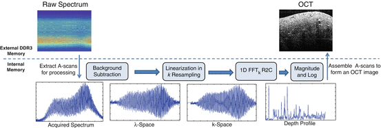

Fig. 14.4
Steps in the OCT signal chain. R2C is real-to-complex
14.4.1 Dataflow
Typically, an acquired OCT frame would be copied from the frame grabber or data acquisition device onto the external memory on the DSP board. The OCT processing can be partitioned in a number of ways using the DSPs. An example is shown in Fig. 14.5 where a single OCT frame is partitioned into several subsets of A-scans and each of these subsets would be operated independently and in parallel by a different DSP core. Within each core, all the processing on the A-scans are done serially, and finally the processed subsets from all the cores are assembled back to form the final processed frame. The partitioning of the frames into subsets can easily be done using OpenMP pragmas as shown in Fig. 14.6.
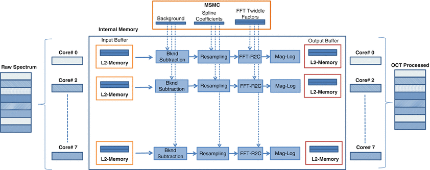


Fig. 14.5
OCT implementation on the multi-core DSP

Fig. 14.6
Partitioning of OCT frames through OpenMP pragma
In principle, all processing on the data can be performed with the data residing in external memory. However, it is preferable to do the data-intensive operations by moving the data into the fast internal memory available on the DSP chip itself. Often it would be necessary to further divide the data subsets (that have been assigned to each core) into small enough patches that can fit within the limited amount of available internal memory. Each of these patches would contain several A-scans depending on the initial frame size, the number of available cores, and the amount of available internal memory. Each patch once moved inside the internal memory can be accessed at high speeds and, after completion of the processing, is copied back to the external memory. This additional overhead due to memory transfers between the external and internal memory can be minimized using direct memory access (DMA) controllers which can overlap the data transfer with data processing. Typically, memory buffers are configured in the internal memory and are operated as ping-pong buffers (double buffering) to overlap data transfer with the processing. An example of this dataflow within a single core is shown in Fig. 14.7, where the data subset assigned to the core is divided into patches and moved into the internal memory using the DMA controller. Four buffers each of which has a size equivalent to a single patch are configured in internal memory and are used for input, output, and processing purposes. As the Nth patch is being processed by utilizing the processing buffer (and temporary buffer for holding intermediate values), the (N – 1)th patch is copied back to the external memory from the output buffer after undergoing processing in the previous iteration. At the same time, the (N + 1)th patch is being copied into the input buffer, which would be processed in the next iteration. These buffers are then interchanged at the end of each iteration and hence are used alternatively for input, data processing, and output tasks. This procedure continues until all the N patches within the core have been processed.


Fig. 14.7
Dataflow through buffers for OCT/ISAM implementation
14.4.2 OCT Data Processing on the DSP
Several chapters in this book present OCT processing methods in detail. Therefore, in this chapter, we will only focus on DSP implementation of standard OCT processing tasks which primarily include resampling and Fourier transform operations. In OCT, several inputs such as background spectrum, resampling indices, and the twiddle factors for the fast Fourier transform (FFT) can be precomputed. These precomputed values will need to be accessed by all the A-scans in each of the cores; hence, it is generally preferable that they be stored in a global memory with fast access times. One such option is utilizing the MSMC.
14.4.2.1 Resampling
The acquired spectrum measured by the spectrometer or obtained from swept-source OCT systems is a function of wavelength, hence, making the λ-k resampling a necessary step in OCT processing. A variety of interpolators (e.g., linear, cubic B-spline) have been employed by different OCT groups to perform the resampling. There is always an inherent compromise between the computational complexity and image quality of the different interpolators employed. Cubic spline interpolation, however, remains a relatively popular interpolator and its implementation on the DSP will be discussed here.
The resampling indices can be computed using a third-order polynomial function:  , where ω ctr is the center wavelength and N is the number of points in a single A-scan. The nonlinear mapping between the k-domain and the wavelength is adjusted using the parameters β2 and β3. These parameters are used to compute the integer and fractional parts that can be subsequently used to determine the spline table coefficients. The resampling indices/spline table coefficients, however, only need to be calculated once in the initialization phase, and the same indices can be reused for resampling every A-scan.
 , where ω ctr is the center wavelength and N is the number of points in a single A-scan. The nonlinear mapping between the k-domain and the wavelength is adjusted using the parameters β2 and β3. These parameters are used to compute the integer and fractional parts that can be subsequently used to determine the spline table coefficients. The resampling indices/spline table coefficients, however, only need to be calculated once in the initialization phase, and the same indices can be reused for resampling every A-scan.
In our implementation, we have followed the technique described in [19]. Prior to using the interpolator, first-order causal and noncausal infinite impulse response (IIR) filters were employed to prefilter the data. This prefiltering is necessary to obtain an exact interpolated value at the original sampling indices. A first-order causal IIR filter, i.e., b k = x k + αb k−1, would require that the previous output value be available before the current output value can be computed. This operation is inherently serial in nature. Implementation of straightforward IIR filtering cannot take advantage of the parallelism available inside a core through the availability of multiple compute units and SIMD instructions. In order to improve the parallelization of computations, the equation b k = x k + αb k−1 was unrolled to up to three levels, as shown below.


